Basics of Semiconductor Manufacturing Process
Semiconductor fabrication is a complex process with hundreds of steps involved. Continuous demand for faster and more energy efficient chips is fueling the creation of smaller transistors and denser chips. This drive for miniaturization poses huge manufacturing challenges requiring new science, new materials, new semiconductor equipment and new ways of thinking. For the uninitiated, or newcomers in the field, the entire process seems mysterious. I hereby present the basic semiconductor manufacturing process.
SEMICONDUCTOR MANUFACTURING PROCESS
Emmanuel Epie
3/23/202510 min read
Introduction:
Electronic devices such as computers, mobile phones, smart watches, etc. have greatly improved our quality of life lives and productivity. Most businesses, governments, military, banks and airports, just to name a few, will grind to a halt if critical computer system (software/hardware) fails: We saw this recently with the Microsoft smiley face blue screen event that disrupted activities across the globe leading to flight delays and loss of productivity at the work place.
The brain of every electronic device is the microprocessor consisting of billions of tiny switches called transistors that transmit signals by switching between on (1) and off (0) states. These transistors are instructed by programs written by computer scientists/programmers. Chips with smaller and highly dense transistors are generally faster and more energy efficient: desirable properties for AI systems. It is no secret that AI is revolutionizing the way we do business. AI systems work by rapidly processing large amounts of data to produce accurate results. These AI systems are also energy and memory hungry as the amounts of data they process are extremely large and so much energy is required to cool them down. There is, therefore, a great need for faster and more energy efficient chips. One way of achieving this is to continue shrinking transistor sizes and increasing their density on a chip. Other approaches include developing new materials, new integrated circuit designs/architectures or combinations of both. This article assumes the reader is familiar with basic transistor physics. A useful refresher can be found at https://byjus.com/physics/mosfet/.
To reduce transistor sizes and increase their density per chip, transistor architecture has evolved from PlanarFET (MOSFETs) to three dimensional fins (FINFET) and recently gate all around FET (GAAFET) where the channels can be shapped as nanowires or nanoribbons (RibonFETS or MBCFET). Nanowire channels are rounder than nanosheets as shown below. The more gate surface area contacting the channel, the better the device performance and the smaller the device footprint. The manufacturing process has also advanced as each of these architectures (generations) come with major technological challenges and unique combination of new and existing fabrication steps. Each manufacturer has developed their own proprietary techniques to address these challenges. Below are the basic semiconductor manufacturing processes. As you will realize, some of these steps are repeated several times within the process flow.

Czochralski process for silicon fabrication. (Credit: João Lucas de Souza Silva)
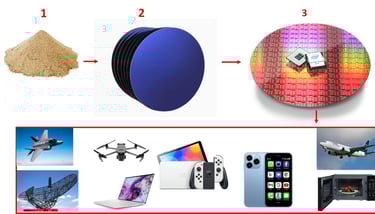
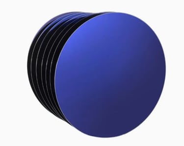
Sliced polished and cleaned silicon safers. (Credit: https://hncrystal.en.made-in-china.com/)
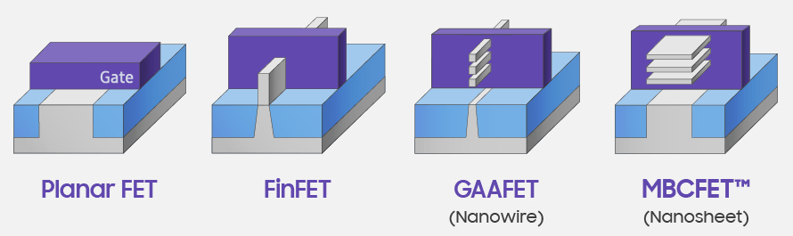
As we move from planar (MOSFET) to gate all arround (GAA) transistors (i.e. NanoFET or RibonFET), gate surface area contacting the channel increases, leading to better device performance. (Credit: anandtech.com)
source
Drain
Gate
Gate
Gate
source
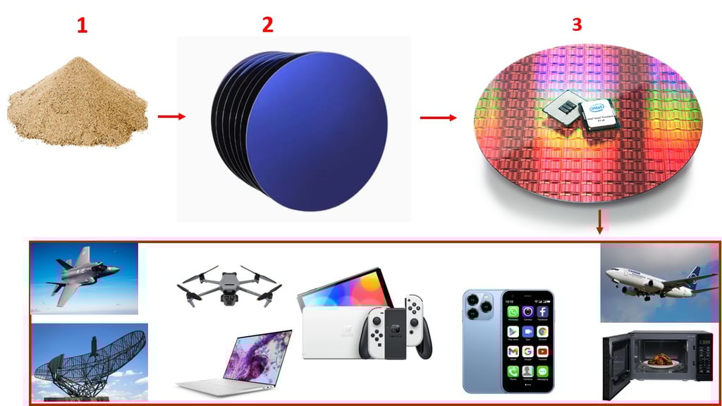
I. Wafer Manufacturing
Silicon is the foundation for most semiconductor manufacturing. Sand is heated until it melts into a pure liquid. The molten sand is then carefully pulled out to cool and crystallize into a single crystal cylindrical rod called an ingot (or boule). This method of Si fabrication is called the Czochralski Process. The Si boule is further sliced into thin circular silicon wafers. The sliced wafer surfaces are rough and contain defects which are not suitable for device fabrication. To eliminate surface roughness, sliced Si wafers are polished and cleaned. Exposure of Si to ambient conditions leads to the growth of a nonuniform native oxide layer on the surface. This oxide layer must be removed before starting device fabrication.
II. Pre-Clean
Before entering the fabrication process, a water's surface must be cleaned to remove the native oxide, adhering particles as well as other impurities (organic/inorganic). Cleaning also improves surface adhesion during deposition thereby improving yields and overall device performance. This cleaning process generally uses:
a) Solvent cleaning methods, e.g. Piranha which is a combination of Sulfuric Acid, Hydrogen peroxide and deionized water. Solvent cleaning is the most widely used silicon cleaning method because of its effectiveness.
b) RCA cleaning which is a combination of one or more solvent cleaning methods inside a warm ultrasonic bath consists of mainly:
1. SC - 1 (standard clean 1): basic solutions for organic defect removal
2. SC – 2 (standard clean 2): acidic solutions for inorganic defects removal
c) Dry cleaning methods which include techniques like:
1. Ozone cleaning: wafers are immersed inside an ozone plasma which reacts with organic defects forming gaseous byproducts like carbondioxide which are socked out of the chamber, thereby cleaning the surface.
2. Laser cleaning: uses laser beams to lift or ablate contaminants, leaving the wafer surface relatively undamaged.
3. Cryogenic cleaning: wafers are rapidly chilled at cryogenic temperaturesand the defects removed by light brushing or rinsing.
Nowadays, cleaning happens in multiple steps. In fact, 30 – 40% of current semiconductor manufacturing steps are cleaning related. Without proper cleaning, yields will be too low as the size of killer defects continues to shrink with transistor sizes in moderntechnology nodes. Low yields mean the semiconductor manufacturer will not be able to make profits. Further details on Si clean will be presented in a separate article. LAM Research is a major manufacturer of cleaning tools.
III. Oxidation
Once wafers are cleaned, they go through a controlled oxidation process that grows a thin oxide layer on the wafer surface. In this process, oxygen or wafer vapor is sprayed on the wafer surface to form a uniform oxide film. This oxide film protects wafer surfaces and insulate neighboring circuits from leakage current. In advanced nodes like FinFET and RibonFETS with smaller dimensions, this Silicon oxide layer breaks down electrically and is replaced by high dielectric material like Hafnium Oxide.
IV. Photolithography
The purpose of photolithography is to print circuits on the wafer. Here, Si wafers are spin coated with a photoresist (photosensitive chemical) film and baked in an oven. Light is then shown on the wafer through a photomask for the desired circuit. The wafer is now sprayed with a developer to remove unlit areas. The patterned wafer is inspected to ensure proper patterning. If it fails inspection tests, the entire pattern is removed, the wafer cleaned and the process repeated again. This process is repeated multiple times during semiconductor fabrication as more and more layers get added to the semiconductor. The wavelength of light used is critical as it determines transistor size. Smaller transistors require light with smaller wavelengths. As we continue pushing the boundaries of transistor size/density in keeping with Moore’s law, it is becoming difficult to generate smaller wavelengths of light for the photolithography process. ASML has figured out ways to generate 13.5 nm wavelengths for photolithography and they continue to push the boundary to even smaller wavelengths. Their costly Extreme Ultraviolet (EUV) systems have cemented ASML’s reputation as aglobal photolithography equipment manufacturing giant. It is no longer possible to fabricate advanced nodes like 7 nm and below without these ASML EUV machines. Needles to say that these machines are complex, difficult to manufacture en mass and are heavily capital intensive. Only a handful of semiconductor manufacturers like Intel, TSMC and Samsung can afford them.
V. Etch
Etch is the selective removal of materials from a wafer surface. Depending on the technology requirements, it can be achieved using wet chemistry, reactive plasma or physical sputtering. After lithography, the exposed thin film layer is etched out by wet (liquid) or dry (gas or plasma) etching process. Like photolithography, etch is repeated multiple times during the semiconductor fabrication process since more layers are continually added and removed. Etch is an especially important process in semiconductor manufacturing and has advanced to the stage where single atoms can be selectively removed with great accuracy and precision. This is particularly important for the fabrication of nm and Angstrom sized transistor/devices. LAM Research has established itself as a major player in semiconductor etch tools/equipment manufacturing.
VI. Deposition
Thin filmlayers are deposited to impart specific electrical or physical characteristics such as protecting the stack circuit layers from shorting or creating a conductive path. This is done using methods like atomic layer deposition (ALD), chemical vapor deposition (CVD), molecular layer deposition (MLD), and electrochemical deposition (ECD). Other reasons for deposition in semiconductor manufacturing includeproviding a diffusion barrier, improving adhesion of subsequent layers, etch stop and provision of anti-reflection coatings. Major deposition tool suppliers are LAM Research, Vapor Technologies Inc., PVD Products, Blue Wave Semiconductor, Veeco Instruments, Inc…etc.
VII. Ion Implantation
Silicon is bombarded with ions to change its electrical properties, roughen its surface to improve thin film adhesion, armophize the subsurface to modify its physical properties depending on the technological needs. Silicon is given excess electrons (n-type Si) after bombardment with a pentavalent element like Phosphorus or Arsenic. Silicon is equally made electron deficient (moreholes) after bombardment with a trivalent element like Boron leading to what is called p-type silicon. A transistor is formed. It is important to note that resistcan also be bombarded with Si or other atoms to minimize edge bias. Leading implant equipment manufacturers include Applied Materials, Axcelis Technologies, Sumitomo Heavy Industries Ion Technology Co., Ltd. (SHI), Nissin Ion EquipmentCo., Ltd, ULVAC Technologies and Ion Beam Services (IBS).
VIII. Metallization
Thin metal layers are deposited to connect the transistor source, drain and gates. For current to flow from a transistor’s source to its drain, the gate must either be switched on or off depending on thetransistor configuration. To further ensure communication between transistors, additional metal layers (wiring) are added through a combination of repeated etch and deposition steps. Once the final metallayer is deposited, a passivation layer is added followed by solder bumps to provide electrical contact between the die and the package. A die is the fundamental building block of an integrated circuit. Each semiconductor wafer at this stage consists of an array of dies physically and electrically separatedfrom each other by a path on its four sides. These dies (or dice) may be evaluated at this stage in a process known as wafer sort, or they may be separated (singulation), picked and assessed in a process known as die sort. Leading semiconductor metallization equipment manufacturers include LAM Research, KLA Corporation, Hitachi, ASM, ULVAC Inc., and Plasma-Therm LLC.
IX. Chemical Mechanical Planarization
Chemical Mechanical Planarization or Chemical Mechanical Polishing (CMP) is a crucial step in semiconductor manufacturing, that uses a combination of chemicals and mechanical forces to remove excess material and smooth layers post deposition. It ensures semiconductors achieve highly uniform and defect free layers. The wafer is pressed against a rotating polishing pad in the presence of a slurry containing abrasives and chemicals. These chemicals soften the material so that the mechanical abrasion can easily remove it. The rate of removal is proportional to applied pressure, temperature and relative rotation speed of wafer and pad (rotating surface on which wafer is pressed against). The result is a planarized surface. Steps are taken to ensure thickness uniformity and address common defects like scratches, particles, residues and domes. CMP is essential for achieving multilevel metallization in integrated circuits. CMP is repeated after the deposition of each layer. Key manufacturers of CMP toolsets are Entrepix, Applied Materials, Stahli USA, Ebara and Precision Finishing. Major pad and slurry manufacturers are Entegris, 3M and Dupont.
X. Die Prep
This is the stage where wafers are thinned and dies separated using lasers and saw tools. The separated dies are then inspected for physical defects, picked and placed into trays for electrical testing.Sometimes, depending on the application, dies may be coated with a thin metal film on the backside for efficient heat spreading/cooling. Leading Die Prep equipment manufacturers include Disco, ASMPT, Samco Inc., Daitron, KLA Corporation and LAM Research.
XI. Sort
All Singulated dies are then tested electrically using hot and/or cold sockets. The purpose is to filter out bad dies prior to packaging, collect yield data to track factory performance or simply to segment dies into categories based on die characteristics for pricing. Leading semiconductor die sort equipment manufacturers include Syagrus Systems, 4JM Solutions and NDC International,
XII. Packaging
After sort, dies may be bonded directly tosubstrate with electrical led attached or bonded to other dies horizontally through Intel’s EMIB or vertically through Intel’s FOVEROS packaging technologies. Other advanced packaging techniques include TSMC’s CoWoS. Molding then completes the packaging. Marking is printed on the package mold to identify the chip (packaged die) designer (e.g. Samsung, Intel, NVIDIA) as well as critical information such as serial numbers. Semiconductor packaging is a multistep process with multiple toolsets involved. Top semiconductor packaging equipment manufacturers include ASMPT, AMAT, ASML, LAM Research, KLA, Tokyo Electron (TEL), Teradyne, Adventest, and Edwards.
XIII. Final Testing
Chips are re-evaluated for shorts, opens, and other characteristics. At this stage, chips are also subjected to accelerated aging conditions such as elevated temperatures (125+ degrees Celsius) and voltages for a specific duration (48 to 168 hours) to remove early failures(infant mortality) induced by manufacturing defects or weak components. This improves reliability, reduces field failures, enhances quality, and saves shipping/storage cost.
XIV. Distribution
Good chips are then shipped out to customers like DELL, LENOVO, Amazon, Alibaba, Microsoft, Apple, the military, aircraft manufacturers,…etc. to embed in their systems before selling to consumers around the world. Now you know how your computer or mobile phone chip is fabricated.
This is a high-level summary of the semiconductor fabrication process. For simplicity, I have only highlighted major processes and have excluded metrology steps involved in each of these processes. It suffices to say that each semiconductor fabrication process involves multiple inline metrology steps used to gauge the line and process health. It takes on average 6-8 months to transform a bare silicon wafer into a functional chip. These processes require pinpoint accuracy and a very clean atmosphere, as a single dust particle may kill a device. That is why semiconductor engineers are dressed in bunny suits, to prevent us from contaminating wafers in process. Additionally, dangerous chemicals and machines are used in the semiconductor fabrication process, requiring the use of PPE like safety glasses and sometimes hazmat face masks. Semiconductor engineers are trained to prioritize safety, execute flawlessly and pay attention to details. Semiconductor fabrication is an exciting job where continuous learning and innovation is key.
Hopefully, this gives you a sneak peak into the semiconductor manufacturing world. Feel free to share your feedback through email at info@quovitek.com. Like and follow our LinkedIn page for more interesting articles.
Glossary of terms:
Die: A small square piece of semiconductor material on which a functional electronic circuit, such as a microprocessor, is fabricated.
Moore's Law: the number of transistors in an integrated circuit doubles every two years.
Technology node (also process node or simply node) often refers to transistor size and design rules.
Tool: Semiconductor equipment.

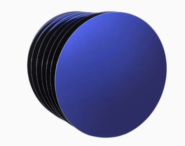
Intel former CEO, Pat Gelsinger, holding up Emerald Rapids in his right hand and Meteor Lake in his left hand. Wafers infront of him L-R: Luna Lake (client computing), Granite Rapids (data center), Siera Forest (data center), Arrow Lake (client computing). Notice individual dies visible as square grids on the wafer surface. (Credit: Intel)
source
Drain
If you enjoy our content and wish to support with a cup of coffee, click this support button. Thanks!


Quovitek Consulting LLC
Helping Manufacturers Thrive
info@quovitek.com
(832) 662-3581
Designed and built by: Epie and DizzySolutions © 2025. All rights reserved.