Fundamentals of Silicon Wafer Cleaning Processes
Silicon, known for its abundance and ease of use, stands as the most widely used semiconductor substrate. The demand for smaller devices with increased transistor density highlights the criticality of maintaining defect-free surfaces, as even a nanometer-sized defect can render a device inoperable. Efficient silicon wafer cleaning plays a pivotal role in ensuring high yields, enhancing device quality, and optimizing performance. Notably, cleaning processes represent a substantial portion, ranging from 30% to 40%, of the contemporary semiconductor fabrication process, underlining its significance as a focal point of ongoing research. Here, I elucidate the essential principles governing silicon wafer cleaning processes in semiconductor manufacturing.
SEMICONDUCTOR MANUFACTURING PROCESS
Emmanuel Epie
5/25/20254 min read
Introduction
Silicon is the most widely used semiconductor substrate because of its relative abundance, ease of processing, ability to form high quality insulating oxide layers and suitability to a wide range of electronic applications. It provides the foundation on which various electronic components like transistors, resistors, capacitors and other components are built. The overall performance, quality and reliability of these components and the chip depends on the quality of wafers used. Before silicon wafers enter the fabrication process, their surface must be cleaned to remove
adhering particles
impurities (organic/inorganic) and
Silicon native oxide
using various cleaning methods or processes. The goal is to remove particles/impurities without altering the underlying substrate properties. These cleaning processes continue throughout the fabrication process. For example, silicon wafers are cleaned pre-diffusion to remove metallic ions which if allowed to diffuse into the wafer will impact its conduction properties. Equally, silicon wafers are cleaned post etch to remove residual photo resist and polymers.
Due to shrinking transistor sizes, the negative impact of defects on dies has increased in severity. Nowadays, few nm size particles can kill a die, hence the name “killer” defects. Silicon wafer cleaning is the removal of particles and chemical contaminants without altering or damaging the wafer surface/substrate. Cleaning has become increasingly important with advanced technological nodes and makes up 30 - 40 % of the total chip manufacturing process.
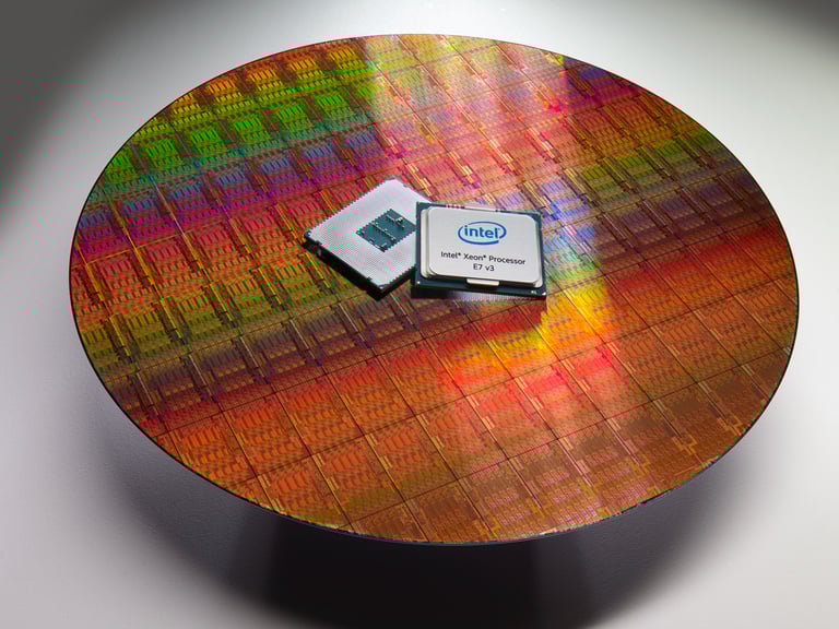
Credit: Intel
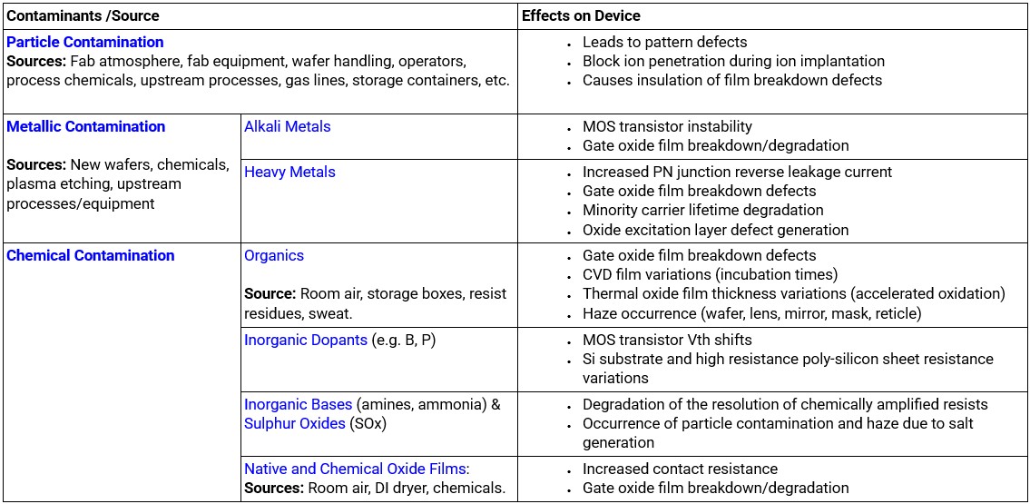
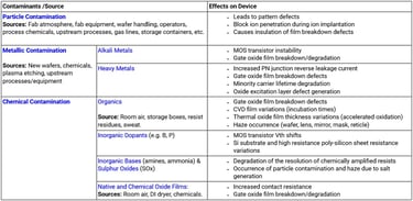
I. Impact of Common Si Surface Defects on Device
II. Benefits of Silicon Cleaning
Removes native oxides
Removes defects/contaminants which can degrade performance or kill a die
Improves surface adhesion during deposition
Improves process yield and device performance.
Reducing wafer scraps, thereby saving cost.
III. Silicon Cleans Process: Wet and Dry Cleaning Methods
Nowadays, cleaning happens in multiple steps. In fact, almost every defect sensitive semiconductor process step involves a form of cleaning. Some of these steps include:
Deposition
Etch
Implant
Planarization
Packaging
Before and after cleaning, it is important to assess the existing contaminants and the effectiveness of our cleaning method. A common way of doing this is by including Pre/Post Clean Metrology steps. This also ensures the cleaning process does not introduce its own defects. Common metrology used are:
Surfscans, AFM, TEM: The wafer surface is scanned to provide surface particle/contaminants count, size and distribution across the wafer. Also measures surface roughness.
EDX, XPS, FIB-SEM, IRLC: Identifies elemental composition of defects/contaminants.
Once we know the nature of contaminants, we can then choose the most suitable cleaning method. Two broad approaches commonly used to remove surface defects in semiconductors are solvent (wets) cleaning and dry-cleaning methods.
1) Solvent (Wet) Cleaning:
The use of solvents to remove impurities on silicon wafer surfaces is considered the most effective approach. This method uses various solvents to remove particles and contaminants from the silicon surface. In some cases, solvent cleaning is performed under warm temperatures in an ultrasonic bath to increase its effectiveness.
Ultrasonic/Megasonic cleaning uses high frequency (0.8 – 2 MHz) vibrations to generate cavitation (low pressure) bubbles on the wafer surface while submerged in a solvent. These bubbles scrub the silicon surface and penetrate difficult geometries, removing contaminants. Choosing the right power settings and vibration frequency is important to avoid damaging wafers.
The table below summarizes common defects, and the various wets methods used to clean them.
2) Dry Cleaning:
These are non-solvent wafer cleaning methods. They are compatible with existing fabrication processes and are more environmentally friendly as few chemicals are needed. However, they are less effective compared to solvent cleaning methods. But there is ongoing research to improve their efficacy. Common examples include Laser cleaning, Cryogenic cleaning, Oxygen/Plasma cleaning
a) Laser Cleaning:
Here, the wafer surface is exposed to a laser that eliminates contaminants by lifting them. Inert gas is then blown over the surface to sweep away the impurities. This might induce slight surface roughness on the wafer surface. This method is effective in removing photoresist films, metallic ions, and chemical impurities.
b) Cryogenic Cleaning:
The contaminated silicon wafer is rapidly chilled to low cryogenic temperatures embrittling the contaminants. Light brushing or rinsing causes the particles/contaminants to flake away. This method prevents contaminants from adhering or diffusing into the substrate.
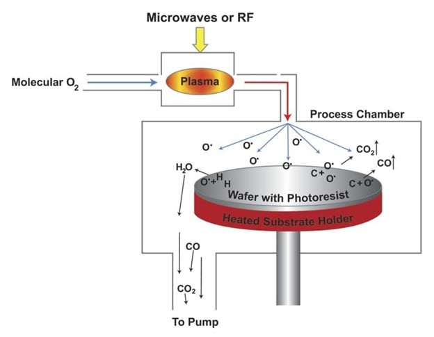
c) Oxygen Plasma Etching:
This method is ideal for removing organic impurities and for increasing the silicon surface wettability. The wafer surface is exposed to an oxygen plasma made of unstable reactive ions/radicals which reacts with surface contaminants (organics) to produce volatile products like CO2 which can be scrubbed out of the chamber. This method is ideal for photoresist striping and improves sidewall profiles. Plasma cleaning is highly repeatable, relatively less expensive, and can be done on a wide variety of materials compared to wet cleaning. However, this process also oxidizes the substrate.
Oxygen plasma cleaning process. (Credit: mks.com)
IV. Conclusion
Cleaning is a crucial part of semiconductor fabrication as it removes defects thereby increasing yields and device performance. Broadly speaking, silicon cleaning can be classified as solvent (wet) cleaning or dry cleaning. Solvent cleaning, although not very environmentally friendly as dry cleaning, is the most effective and widely used in the semiconductor industry. Cleaning comprises 30 – 40 % of the semiconductor fabrication process and its importance continues to grow with the push for device miniaturization.
References:
1) Binoy Bera. Silicon Wafer Cleaning: A Fundamental and Critical Step in Semiconductor Fabrication Process. International Journal of Applied Nanotechnology. 2019; 5 (1): 8 – 13p
2) Karen A. Reinhardt and Werner Kern. Handbook of Silicon Wafer Cleaning Technology. Materials Science and Process Technology Series. 2018
3) https://www.inrf.uci.edu/wordpress/wp-content/uploads/sop-wet-silicon-solvent-clean.pdf

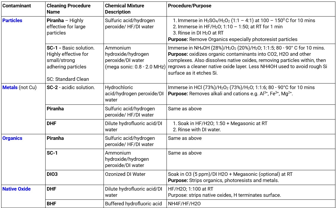

A combination of Standard Clean (SC) and/or Piranha methods is sometimes refered to as RCA cleaning.
If you enjoy our content and wish to support with a cup of coffee, click this support button. Thanks!


Credit: SK hynix
Quovitek Consulting LLC
Helping Manufacturers Thrive
info@quovitek.com
(832) 662-3581
Designed and built by: Epie and DizzySolutions © 2025. All rights reserved.